About the thin film growth chamber
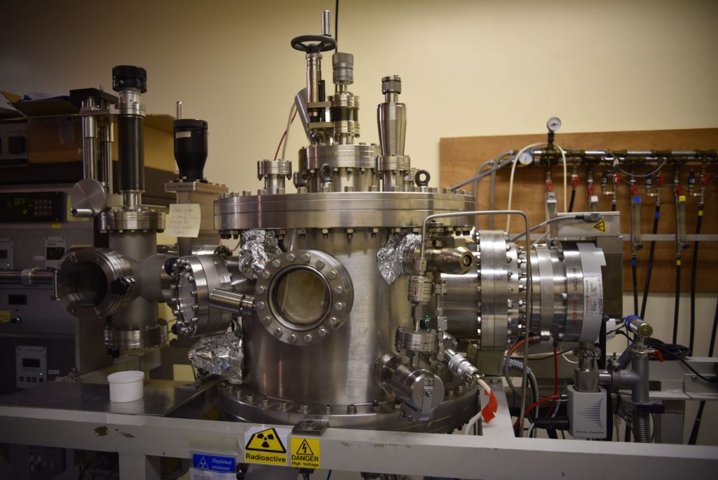
The system has the following capabilities:
- Four DC magnetron guns allow deposition of material individually, sequentially, or simultaneously, to fabricate single element systems, complex multilayer structures or binary/ternary compounds and alloys.
- Range of high purity targets including, but not limited to: depleted U and Th, as well as Al, Ba, Co, Cr, Cu, Fe, Hf, Ho, Ir, Mg, Mo, Nb, Ni, Pd, Sc, Si, Sm,Ta, Tb, Ti, W, V, Yb, Zr. Typical deposition rates < 1 Ås-1, allowing films of thicknesses in the range Å to micrometre.
- Sputtering via inert Ar gas.
- Several additional gas-inlet ports for reactive sputtering, which allows for the deposition of oxide, nitride, and hydride compounds.
- In-situ reflection high-energy electron diffraction to monitor the crystallinity and strain of the substrate and thin film structure.
- Experience with growth on a range of commercial substrate materials from glass and oxidised silicon for polycrystalline or textured samples, to sapphire, YSZ, LSAT, CaF2, SrTiO3 and other single crystals for epitaxially-related growth.
- Load-locked UHV chamber with main chamber base pressure in the 10-10 mbar range.
- Residual gas analysis via a quadrupole mass spectrometer to analyse the sputter gases and composition at base pressure.
- Uniform growth across a substrate size up to 25 mm diameter.
- Substrate temperatures currently up to 900 °C – shortly to be upgraded to > 1000 °C.
About the XPS system
The system is expected to have the following capabilities:
- Lateral scanning with resolution in the tens of microns.
- Ar cluster source system for depth profiling (expected < 0.3 Ås-1).
- Loadlock and UHV connection to the thin film growth chamber.
- Auger detector for reliable, quantitative elemental compositional analysis.
More details will follow as the system is purchased and installed.